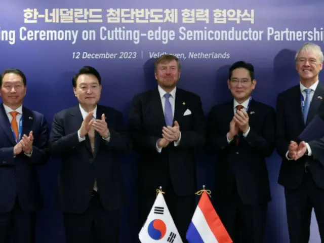
) was announced. As a result, the two companies will jointly invest 1 trillion won (approximately 110,519,900,000 yen) starting in 2024 to establish and operate an R&D center for next-generation semiconductor manufacturing technology in South Korea.
Ru. The two companies will jointly develop ultra-fine processing technology using next-generation extreme ultraviolet (EUV) light. Surpassed Taiwan Semiconductor Manufacturing Co., Ltd. (TSMC), the world's largest foundry (semiconductor contract manufacturing)
Therefore, securing EUV equipment is a top priority for Samsung Electronics. In relation to this, an industry official said, ``ASML will have high NA (numerical aperture) at the end of next year.
We plan to start providing EUV equipment "Twin Scan EXE: 5200". In the foundry industry, competition to secure this new equipment is fierce.
"It will become a big deal," he predicted. Samsung Electronics plans to produce semiconductors using a 2-nanometer circuit line width process in 2025 and a 1.4-nanometer process in 2027.
Regarding the establishment of the R&D center, an official from the Korean President's Office said, ``As the first R&D center that ASML will establish overseas together with a semiconductor manufacturer, it has great symbolic meaning.''
We will provide full support from establishment to operation."
2023/12/15 08:26 KST
Copyrights(C) Edaily wowkorea.jp 101

