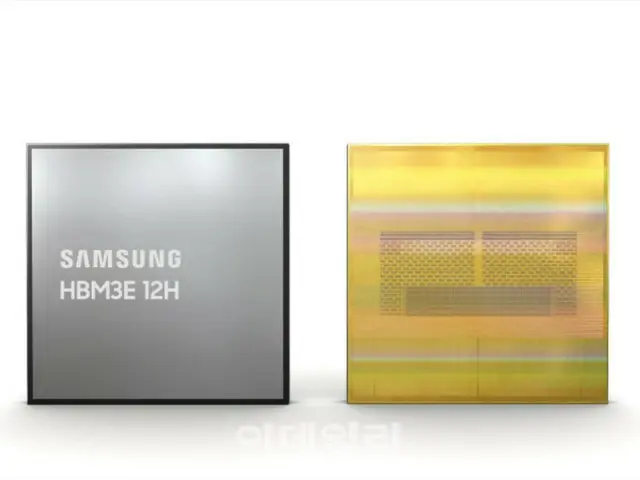
By using through-silicon vias (TSV) in a DRAM chip, we have realized a 12-layer stacked HBM3E (5th generation HBM) 12H (12-layer stacked).
The company will begin mass production of this product from the January to June period of this year. It is scheduled to be supplied together with the 8-layer stacked HBM3E 8H, which was decided to be supplied prior to this.
Samsung Electronics, SK Hynix, and Micron of the US, which hold a large share of the DRAM market, are expected to accelerate the development and mass production of their cutting-edge HBM3E products as early as March.
Micron announced on its website that it had started mass production of the HBM3E. The 24-gigabyte HBM3E 8H (8-tier stacked) product will be shipped from the U.S. Semiconductor University in the April-June period.
It is said to be installed in NVIDIA's image processing semiconductor (GPU) "H200". On the other hand, SK Hynix said, ``HBM3E
8H' mass production began in January. The 12-layer stacked product meets the JEDEC standard for semiconductor devices.
It will be the same height as an 8-tier laminated product." The industry expects that mass production of HBM4 will begin in earnest around 2026.
2024/03/01 08:39 KST
Copyrights(C) Edaily wowkorea.jp 101

